Electronic skin gives robots and prosthetics ‘human-like touch sensing’
Hanyang University ERICA researchers have developed a vertically integrated dual-gate transistor design, which could give robots ‘reliable touch sensing and high density, large-area integration’. Conventional tribotronic devices, that convert mechanical stimuli like touch into electrical signals, offer fixed sensitivity and pose challenges in large-area integration…
Hanyang University ERICA researchers have developed a vertically integrated dual-gate transistor design, which could give robots ‘reliable touch sensing and high density, large-area integration’. Conventional tribotronic devices, that convert mechanical stimuli like touch into electrical signals, offer fixed sensitivity and pose challenges in large-area.
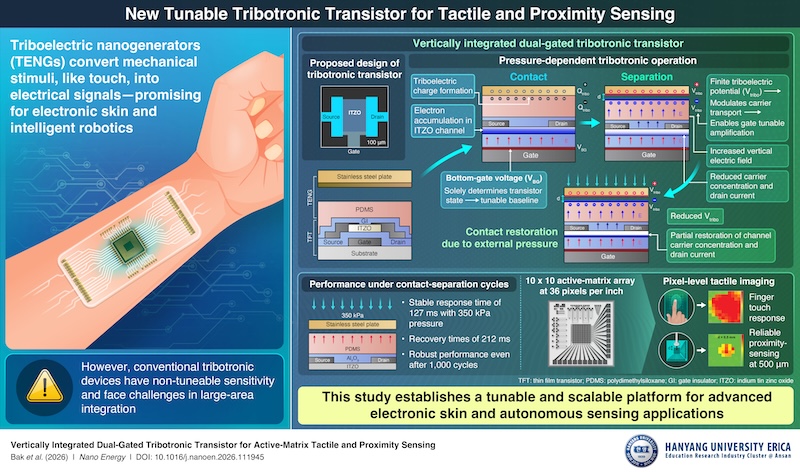
In a new study, researchers have developed a new vertically integrated dual-gated tribotronic transistor architecture, that offers tuneable sensitivity, reliable contact and proximity detection, as well as minimal pixel footprint for high-density array integration. This technology can pave the way for electronic skin systems.
What Happened
The recent advancement of miniaturized and portable electronics, particularly wearable and flexible devices, has increased the demand for self-powered sensing technologies. Among these, triboelectric nanogenerators (TENGs) have received increased attention for developing highly sensitive tactile sensors.
Their study was made available online on April 9, 2026, and published in Volume 153 of Nano Energy on June 15, 2026.
It also maintained stable performance without noticeable degradation after 1,000 operating cycles.
Overall, this innovative architecture provides a scalable platform for programmable, mechanically robust tribotronic sensor arrays, paving the way for advanced human–machine interfaces.
Key Details
TENGs convert external mechanical stimuli into electrical signals through redistribution of electric charges. They are particularly attractive for the development of advanced electronic skin and intelligent robotics.
After initially charging the sensing layer with a stainless-steel plate, they demonstrated pixel-level responses to finger touches as well as reliable proximity sensing at distances of up to 500 micrometers using a stainless-steel probe.
To demonstrate active tactile sensing, the researchers fabricated a 10 × 10 transistor array using the proposed architecture.
Additionally, the device exhibited stable response and recovery times of 127 and 212 milliseconds, respectively, during each contact-separation cycle.
Why It Matters
However, conventional tribotronic devices suffer from non-tuneable sensitivity and pose challenges in integration into large-area architectures, limiting practical applications. To address these limitations, a research team led by Associate Professor Jaekyun Kim from the Department of Photonics and Nanoelectronics at Hanyang University.
The researchers also showed that increasing the contact pressure enlarges the effective contact area between the PDMS layer and the contacting object, generating more triboelectric charge and producing a stronger response.
Specifically, the researchers found that the sensitivity increased with increasing bottom-gate voltage.
What Reports Say
Coverage of the story so far points to:
Continued reporting by Robotics & Automation News as more details emerge